XCT Insights
Stay Updated
Fullerene research, applications and company updates, delivered occasionally.
Latest from XCT
View all


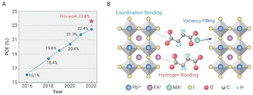
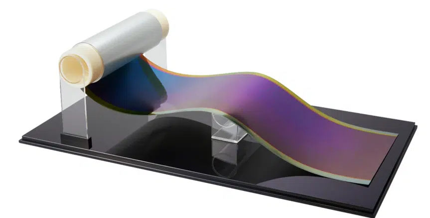
In the rapidly evolving landscape of clean energy, metal halide perovskite solar cells (PSCs) have emerged as a highly disruptive alternative to conventional silicon photovoltaics, demonstrating a meteoric rise in certified power conversion efficiency (PCE) from 3.8% to over 27.0% in less than two decades. To validate the real-world operational viability of this technology, the Japanese government has launched a landmark, government-led demonstration project scheduled to begin in the summer of 2026. This pilot program involves the large-scale deployment of lightweight, flexible perovskite solar cells across various Self-Defense Forces (SDF) facilities, commencing at bases in Okinawa Prefecture. By installing these thin-film modules on diverse building walls and roofs where rigid silicon panels are physically unviable, the project aims to verify the cells’ long-term durability in complex, humid maritime environments and secure energy independence for critical national security infrastructure.
As perovskites transition from laboratory scale to strategic, high-exposure outdoor deployments, the optimization of their internal interfaces represents the most critical barrier to commercialization. In inverted (p-i-n) planar heterojunction configurations—the preferred architecture for tandem integration and roll-to-roll manufacturing due to low-temperature processing and hysteresis-free charge collection—the electron transport layer (ETL) largely dictates both the efficiency and lifetime of the device. Unmodified Carbon 60 (C60) and its soluble derivative [6,6]-phenyl-C61-butyric acid methyl ester (PCBM) have become the undisputed standard interfacial materials to maximize electron extraction and suppress non-radiative recombination.
The dominance of fullerenes as n-type semiconductors in thin-film photovoltaics is fundamentally rooted in their molecular geometry and electronic structure. Unlike planar organic molecules that exhibit highly anisotropic charge transport dependent on face-to-face stacking orientations, the three-dimensional spheroidal conjugation of the C60 carbon cage allows for completely isotropic electron transport. Electrons can tunnel or “hop” with equal probability in any direction across the fullerene domains.
Furthermore, fullerenes exhibit an exceptionally low reorganization energy following electron transfer. This minimised thermodynamic barrier permits ultrafast electron extraction kinetics at the perovskite/ETL interface. In a typical planar cell, the rate constant of photoinduced electron transfer ($k_{ET}$) can be modeled using the semiclassical Marcus equation:
Where $\hbar$ is the reduced Planck constant, $V$ represents the electronic coupling matrix element between the perovskite donor and the fullerene acceptor, and $FCWDS$ is the Franck-Condon weighted density of states. The $FCWDS$ is mathematically defined by the reorganization energy ($\lambda$) and the thermodynamic driving force ($-\Delta G$):
Because $\lambda$ remains remarkably small in fullerenic systems, electron extraction occurs on a sub-picosecond timescale , effectively outcompeting geminate and non-geminate charge carrier recombination. This rapid charge transfer facilitates an efficient charge redistribution at the heterointerface, converting the contact into a highly selective n-type junction that blocks minority carrier holes while collecting majority carrier electrons.
Despite the fast charge extraction mediated by pristine fullerenes, inverted planar PSCs are still limited by non-radiative recombination losses at the perovskite surface and across the perovskite/C60 interface. The surface of polycrystalline perovskite films is inherently populated with localized electronic defects, dominated by halide vacancies, undercoordinated Pb2+ centers, and Pb-I antisites. These surface trap states serve as non-radiative recombination pathways, contributing to severe thermal losses that suppress the open-circuit voltage (Voc) of the device.
To neutralize these active defects, researchers employ multifunctional molecular bridging agents to passivate the perovskite surface while reorganizing the interfacial energetics.
A prominent example is the use of (benzhydrylthio)acetic acid (DSA) to engineer the heterointerface between the perovskite and the PCBM layer. DSA establishes a highly stable molecular-bridging layer through dual-site anchoring. The thioether and carboxylic acid groups of the DSA molecules form strong coordinate covalent bonds with the undercoordinated Pb2+ defect sites, chemically passivating the surface traps. Concurrently, the hydrophobic benzhydryl segment of DSA participates in robust $\pi$-$\pi$ stacking with the overlying PCBM domain. The electron donation from the thioether moiety induces n-type band bending in the perovskite layer, upshifting its Fermi level and creating an enhanced internal electric field that significantly accelerates electron-extraction kinetics.
Similarly, the novel organic bridge NMePS has been designed to reconstruct the surface energetics of inverted PSCs. By tailoring the electronic states at the interface, NMePS drastically reduces the trap state density and yields a highly uniform perovskite surface morphology that is exceptionally receptive to subsequent C60 vacuum deposition. Small-area devices (0.045 cm2) modified with NMePS have achieved a remarkable power conversion efficiency of 26.87%, while larger-area sub-modules (1.00 cm2) maintained a highly stable efficiency of 25.06%. These modified systems exhibit exceptional operational durability, retaining 90% of their initial performance after more than 2,600 hours of continuous tracking.
To completely eradicate interfacial losses, researchers have introduced phenylamino-functionalized ortho-carborane as an ultrathin interlayer between the perovskite and the top C60 ETL. Ortho-carborane possesses a unique three-dimensional spherical aromaticity. The phenylamino groups coordinate with the perovskite surface to passivate defects, while the carborane core acts as a high-mobility electron-transporting and hole-blocking buffer. This dual passivation and blocking mechanism essentially eliminates the interfacial non-radiative recombination, delivering a certified PCE of over 23.0% with an exceptionally low non-radiative voltage loss of only 110 mV. Modified devices retain over 97% of their initial efficiency after 400 hours of continuous maximum power point tracking (MPPT) under simulated solar light.
The fabrication of high-performance p-i-n planar PSCs requires sequential layer-by-layer deposition. This architecture presents a significant processing challenge: when the active perovskite precursor solution is spin-cast, the polar organic solvents required to dissolve the perovskite precursors—most notably dimethylformamide (DMF) and dimethyl sulfoxide (DMSO)—can wash away or erode the underlying electron-transporting fullerene interlayer.
To address this solvent erosion, scientists have synthesized thermally and photochemically cross-linkable fullerene derivatives. Two key derivatives include:
Both cross-linked fullerenes form a robust, highly dense, and solvent-resistant polymer network. Once cured, the C-PCBSD or C-PCBOD interlayers are completely insoluble in nonpolar and polar orthogonal solvents, preventing any material erosion during the subsequent deposition of the perovskite active layer. Furthermore, atomic force microscopy (AFM) has demonstrated that these cross-linked fullerenes provide superior surface coverage over metal-oxide electron selective contacts (such as TiO2 or FTO), passivating oxygen vacancies and interfacial trap states to suppress charge recombination and dramatically elevate the cell’s overall fill factor (FF).
To further refine the electronic coupling at the perovskite/ETL interface, researchers have developed novel C60 derivatives functionalized with thiophene moieties via Bingel reactions. Thiophene-containing addends exhibit a high affinity for the perovskite structure, enabling stronger interfacial bonding through sulfur-metal coordination.
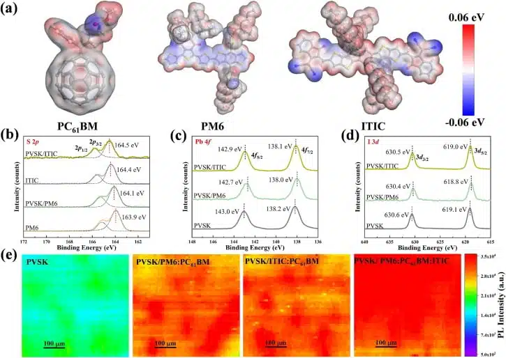
In these customized fullerenes, the addition of electron-withdrawing or electron-donating groups can be used to fine-tune the LUMO levels and band alignment. By comparing bromine (Br) and cyano (CN) functionalized thiophene-C60 derivatives, researchers discovered that while both materials act as efficient electron transport layers, the derivative bearing the highly electronegative cyano group exhibited superior performance. The cyano group significantly increases the local dielectric constant ($\epsilon_r$) of the fullerene interlayer. This elevated dielectric constant screens ionized defects at the interface, reducing trap-assisted recombination and accelerating electron extraction to yield efficiencies that outperform devices fabricated with standard PCBM.
| Interlayer Type | Passivation Mechanism | Voltage Loss Reduction | Stability Metrics | Source |
| PCBM | Weak physical coordination | Moderate | Rapid decay under unencapsulated moisture | |
| DSA-PCBM | Carboxylate-Pb2+ coordinate bonding, pi-pi stacking with PCBM | Significant | Retains 96% of initial PCE after 2000 h MPPT | |
| NMePS | Interfacial energetics reconstruction, upshifted Fermi level | High | T90 > 2600 h at 30 °C, T80 > 500 h at 85 °C | |
| Phenylamino-carborane/C60 | 3D aromatic defect passivation, hole blocking | Supreme (Low Voc loss of 110 mV) | Retains >97% of initial PCE after 400 h MPPT | |
| C-PCBOD | In situ UV cross-linking (45 s), solvent-resistant polymer network | Moderate | Excellent thermal and solvent resilience |
Fullerenes and their advanced engineered interlayers have solidified their position as the premier material class for electron selective contacts in inverted perovskite solar cells. By passivating surface defects, aligning interfacial energy bands, and establishing robust solvent resistance, these carbon nanostructures successfully resolve the dual challenges of non-radiative recombination and structural instability. As global clean energy initiatives drive large-scale, high-exposure pilot tests—exemplified by Japan’s upcoming 2026 military base deployment of flexible PSC modules in Okinawa—the precise molecular engineering of fullerene-based interfaces will remain the central pathway to transition perovskite photovoltaics from a laboratory triumph to a resilient, globally deployed energy source.
C60 is preferred due to its highly symmetric spheroidal geometry, which enables isotropic charge transport. Unlike planar organic molecules, electrons can hop with equal efficiency in all three dimensions through the fullerene domains. Furthermore, fullerenes exhibit an exceptionally low reorganization energy, enabling sub-picosecond electron extraction from the perovskite layer while effectively blocking minority carrier holes.
These bifunctional molecules possess active anchor sites (such as carboxylic acid or thioether groups) that form coordinate bonds with undercoordinated Pb2+ defects on the perovskite surface, passivating surface traps. Concurrently, their conjugated domains engage in strong $\pi$-$\pi$ interactions with the overlying PCBM or C60 layer. This dual-site coupling upshifts the perovskite’s Fermi level and induces n-type band bending, establishing an enhanced electric field that suppresses non-radiative recombination and accelerates charge collection.
In inverted PSCs, the active perovskite precursor is dissolved in highly polar solvents (like DMF and DMSO) and deposited directly on top of the electron transport material. Cross-linkable fullerenes (such as C-PCBSD or C-PCBOD) can be polymerized via thermal treatment or UV light to form an insoluble, solvent-resistant polymer network. This prevents the interlayer from being washed away or eroded during subsequent spin-coating, enabling seamless, layer-by-layer solution processing.
Phenylamino-functionalized ortho-carboranes possess a spherical molecular structure and three-dimensional aromaticity. The phenylamino groups coordinate with surface lead atoms to passivate defects, while the carborane core optimizes the energy alignment at the C60 interface. This combined passivation and hole-blocking effect suppresses non-radiative recombination, reducing voltage losses to a mere 110 mV under continuous operational conditions.
For B2B procurement of Fullerene C60 (Pure), 99.95% Purity, No metallic residue, buyers should confirm target purity, required quantity, application, destination country, COA, MSDS/SDS, packaging, storage conditions, and shipping requirements before requesting a formal quotation.
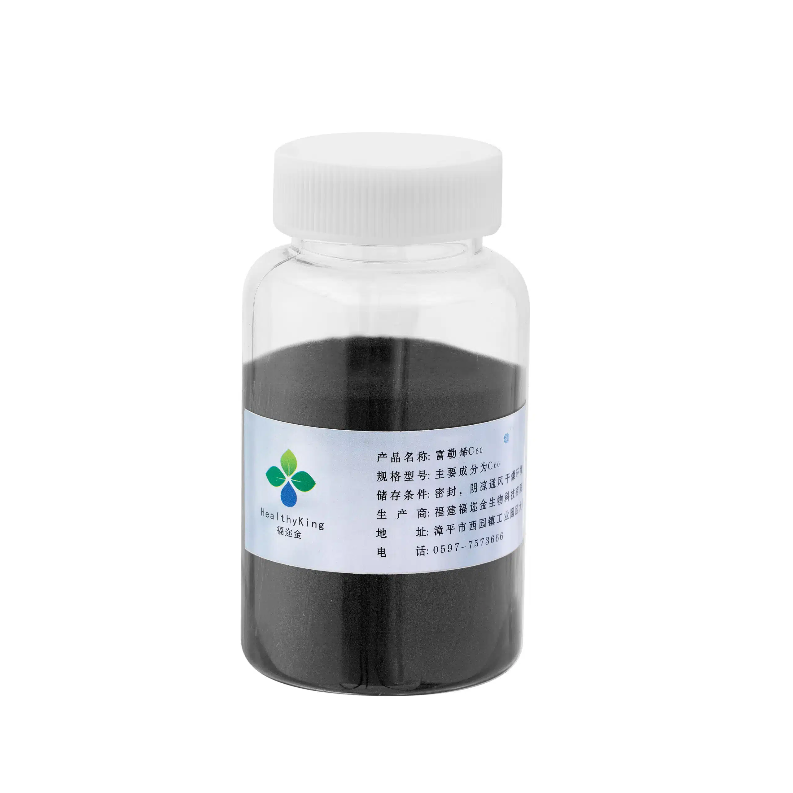
High-purity fullerene C60 is a highly refined nanomaterial designed specifically for the most demanding scientific and industrial applications. This ultra-pure form ensures…
Request product specifications, batch-specific COA, MSDS/SDS, sample availability, packaging details, and international shipping information before confirming your order.
Request DocumentsSubmit your product, purity, quantity, application, destination country, and documentation requirements. Our team will help confirm availability, COA, MSDS/SDS, packaging, and quotation details.