XCT Insights
Stay Updated
Fullerene research, applications and company updates, delivered occasionally.
Latest from XCT
View all
Organic photovoltaics and molecular electronics represent two important directions in advanced organic semiconductor research. Organic photovoltaics, often called OPVs, convert light into electricity through thin organic semiconductor layers. Molecular electronics studies how individual molecules or molecular assemblies can participate in charge transport, memory, switching, sensing, and nanoscale device behavior.
These fields are different, but they are connected by a common material question: how can molecular structure be translated into reliable electronic function?
Fullerene C60, Fullerene C70, and fullerene derivatives such as PC61BM and PC71BM have played a central role in this story. They are studied as electron acceptors, charge-transport materials, interfacial components, molecular anchors, charge-trapping materials, and nanoscale electronic building blocks. Although non-fullerene acceptors have transformed modern OPV performance, fullerene materials remain important in organic electronics because of their electron-accepting behavior, isotropic molecular geometry, and long research history.
The industrial question is no longer whether organic electronics can work in a laboratory device. The harder question is whether these materials can support scalable coating, stable morphology, reproducible charge transport, large-area modules, and supply-chain consistency. This article explains how organic photovoltaics and molecular electronics evolved from molecular innovation toward industrialization, and where C60, C70, and PCBM-type materials still matter.
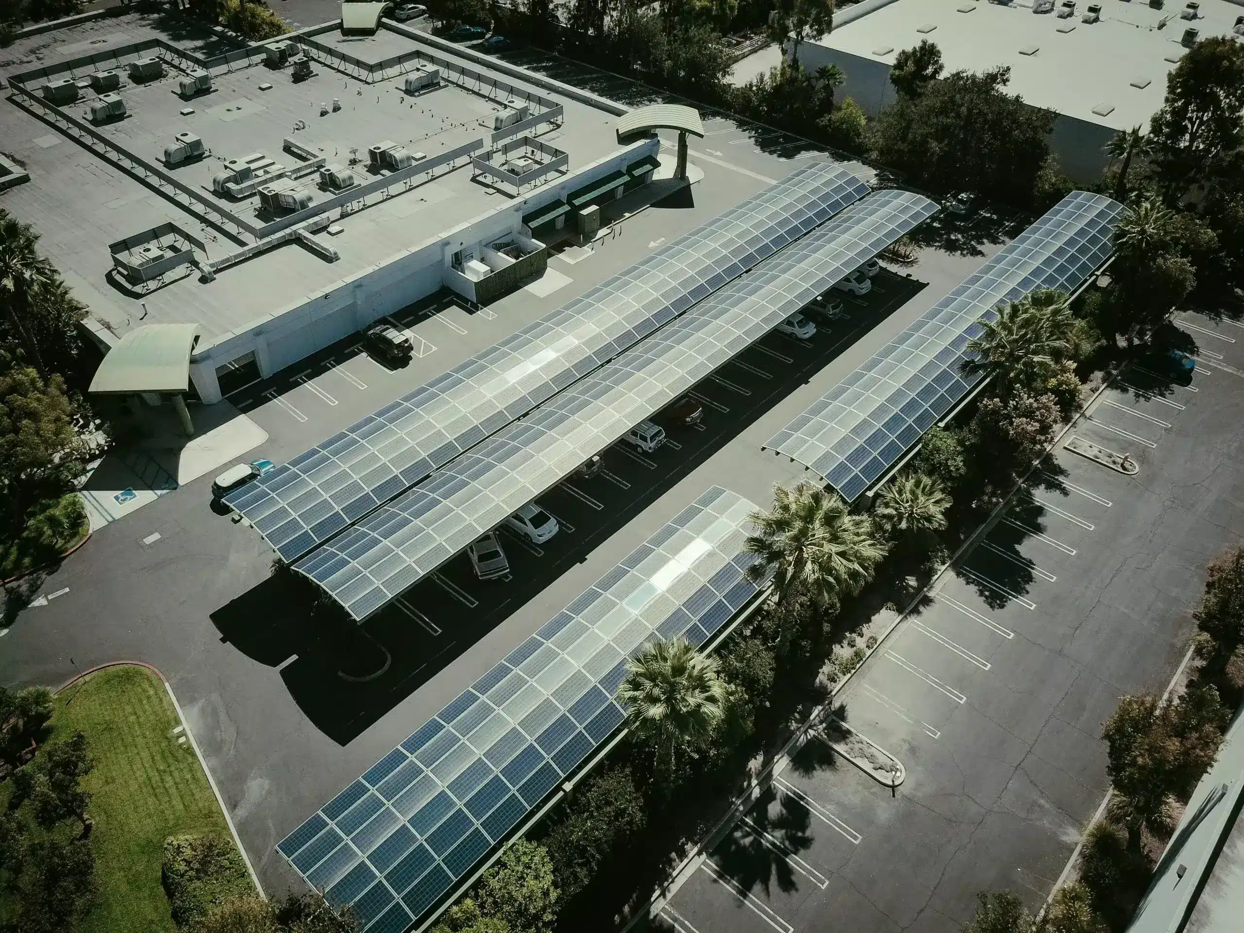
Organic photovoltaics are solar cells based on organic semiconductor materials rather than crystalline silicon. Their value does not come from trying to replace silicon in every solar application. Instead, OPVs are attractive because they can be lightweight, flexible, thin, semi-transparent, and compatible with solution processing or low-temperature deposition.
These properties make OPVs interesting for applications where rigid silicon modules are not ideal. Examples include building-integrated photovoltaics, lightweight portable power, curved surfaces, indoor energy harvesting, transparent or semi-transparent modules, and specialty energy devices. In these areas, mechanical format, weight, optical appearance, and manufacturing compatibility may matter as much as peak efficiency.
OPV technology has improved substantially over the last decade. Small-area laboratory cells based on advanced donor polymers and non-fullerene acceptors have reached much higher efficiencies than earlier fullerene-only systems. However, commercialization depends on more than small-cell records. Large-area coating, module layout, electrode resistance, encapsulation, photostability, morphology control, and manufacturing yield all determine whether OPV technology can move from the laboratory into reliable product formats.
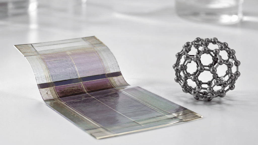
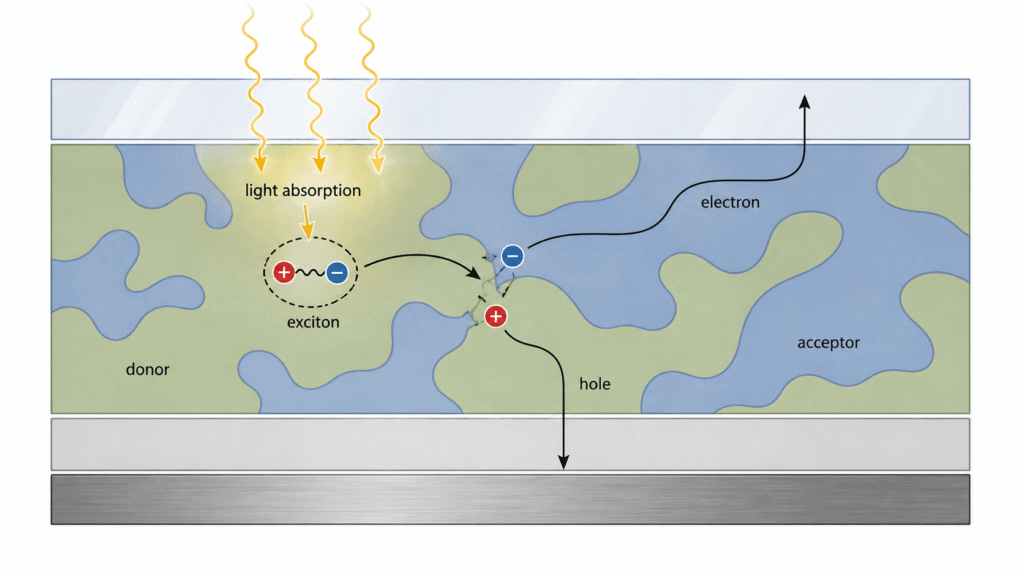
An OPV device converts light into electricity through a sequence of molecular-scale events. First, the active layer absorbs photons. This creates excitons, which are bound electron-hole pairs. Unlike inorganic semiconductors, many organic semiconductors have relatively strong exciton binding energy, so excitons do not automatically separate into free charges.
To generate electricity, the exciton must reach a donor-acceptor interface. At that interface, the energy level difference between the electron donor and electron acceptor helps split the exciton into an electron and a hole. The electron moves through the acceptor phase, while the hole moves through the donor phase. These charges are then collected by the electrodes.
This is why the bulk heterojunction, or BHJ, became a central architecture in OPV research. In a BHJ active layer, donor and acceptor materials are mixed to create a large interfacial area. The goal is to give excitons a high chance of reaching an interface before recombination. At the same time, the donor and acceptor phases must form continuous pathways for charge transport.
The same morphology that makes BHJ devices powerful also creates a commercialization challenge. If the donor and acceptor phases are poorly mixed, charge separation may be inefficient. If they are too finely mixed, charge transport may suffer. If the morphology changes during heat, light exposure, oxygen exposure, or long-term operation, device performance can decay.
Organic photovoltaics and OLEDs both use organic semiconductor materials, but they operate in opposite directions.
In an OLED, electrical energy is converted into light. Electrons and holes are injected from electrodes, meet in an emissive layer, form excitons, and release light when those excitons decay radiatively. The goal is efficient light emission.
In an OPV, light is converted into electrical energy. Photons generate excitons, and the device must separate those excitons into free charges before they recombine. The goal is efficient charge generation and collection.
| Feature | OLED | OPV |
|---|---|---|
| Main conversion | Electricity to light | Light to electricity |
| Primary event | Carrier injection and recombination | Photon absorption and charge separation |
| Role of excitons | Excitons should emit light | Excitons should split into charges |
| Material challenge | Emission efficiency and lifetime | Morphology, charge transport, and stability |
| Device goal | Bright, stable light emission | Stable power generation |
This distinction helps explain why a material that performs well in one organic electronic device may not automatically work in another. OPV materials must be judged by absorption, energy levels, miscibility, morphology, charge mobility, recombination behavior, and stability in a photovoltaic device stack.
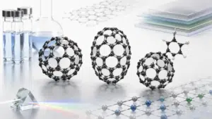
Fullerene C60 is one of the most important carbon molecules in organic electronics. It consists of 60 carbon atoms arranged in a closed cage structure. Its spherical geometry and electron-accepting character made it highly relevant to early OPV research, organic semiconductor devices, molecular electronics, and nanoscale charge-transfer studies.
In OPV research, C60 and fullerene derivatives became important because they could accept electrons from donor polymers and support electron transport. The spherical molecular geometry of C60 also provides relatively isotropic charge-transport behavior, which can be useful in disordered or randomly oriented organic films.
Pristine C60, however, has limited solubility in many processing systems. This is one reason fullerene derivatives became so important. PC61BM, a soluble C60 derivative, allowed researchers to process fullerene acceptors in solution-processed BHJ solar cells. PC71BM, a C70 derivative, later became relevant in systems where broader visible absorption could help improve photocurrent.
Fullerenes are no longer the only important acceptor family in OPV. Non-fullerene acceptors have become dominant in many high-efficiency systems. Still, C60, C70, PC61BM, and PC71BM remain important reference materials and functional components in organic electronics, interfacial research, ternary blends, and molecular-scale device studies.
C60 is the parent fullerene molecule with 60 carbon atoms. It is highly symmetrical and has been widely studied as an electron acceptor and molecular electronic material. In vacuum-deposited organic devices, C60 can be used directly as a thin-film material.
PC61BM is a soluble derivative of C60. Its side chain improves processability in organic solvents, which made it one of the most influential acceptor materials in early solution-processed OPV research. PC61BM helped establish the polymer:fullerene BHJ architecture as a practical device platform.
C70 is a fullerene molecule with 70 carbon atoms. Compared with C60, it has a more elongated molecular structure and different optical behavior. C70 and its derivatives can absorb more strongly in parts of the visible spectrum than C60, which can be useful in some photovoltaic systems.
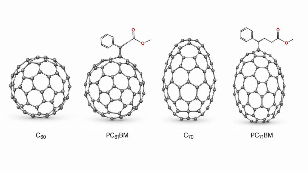
PC71BM is a soluble C70 derivative. It has been used in OPV systems where broader visible absorption is desired. However, C70-based materials should not be described as universally better than C60-based materials. The right choice depends on donor material, energy levels, morphology, processing method, device architecture, and performance target.
| Material | Basic Identity | Main Research Relevance |
|---|---|---|
| C60 | Pristine 60-carbon fullerene | Electron acceptor, vacuum-deposited films, molecular electronics |
| PC61BM | Soluble C60 derivative | Classic solution-processed BHJ OPV acceptor |
| C70 | Pristine 70-carbon fullerene | Organic electronics and photovoltaic research with different optical behavior |
| PC71BM | Soluble C70 derivative | OPV acceptor systems where stronger visible absorption may be useful |
Non-fullerene acceptors, usually called NFAs, changed OPV research by offering stronger absorption, more tunable energy levels, and improved molecular design flexibility compared with many fullerene derivatives. Modern NFA systems can be engineered through fused-ring cores, electron-withdrawing end groups, side-chain design, fluorination, chlorination, and molecular packing control.
The rise of NFAs does not make fullerenes irrelevant. Instead, it changes their role. Fullerene materials are now often discussed as reference acceptors, interfacial materials, additives, morphology modifiers, electron-transport components, or part of ternary blend systems.
This is an important industrial point. A material does not disappear simply because a newer class of materials reaches higher peak efficiency in one device architecture. C60 and PCBM-type materials remain useful because they are well-studied, electronically active, and compatible with several organic electronic research platforms.
In some ternary OPV systems, fullerene derivatives may help tune morphology or provide electron-transport pathways between donor and non-fullerene acceptor domains. The value of fullerenes in these systems must be judged experimentally. They should not be described as guaranteed efficiency boosters, but they remain relevant tools for device engineering.
OPV performance depends not only on the acceptor material, but also on the donor material. Donor polymers and small molecules determine light absorption, hole transport, blend morphology, and energy-level alignment. Common donor design motifs include conjugated backbones, fused aromatic units, electron-rich building blocks, and side chains that control solubility and packing.
Fluorination has become one useful molecular design strategy. Introducing fluorine atoms into donor or acceptor structures can lower energy levels, influence molecular packing, and affect film morphology. In some systems, fluorination can support improved open-circuit voltage, charge transport, or crystallinity. In other systems, it may create processing or miscibility challenges. The result depends on molecular structure and device architecture.
One important concept is molecular orientation. In thin films, organic semiconductor molecules may prefer edge-on, face-on, or mixed orientations relative to the substrate. For solar cells, vertical charge transport to the electrodes is critical, so morphology and orientation can strongly influence current density and fill factor.
This is why OPV industrialization cannot rely on material selection alone. Coating conditions, drying dynamics, solvent systems, additives, annealing, layer thickness, and substrate design all influence the active layer. The same donor-acceptor pair may perform differently when processed by spin coating in a small laboratory cell versus blade coating, slot-die coating, or roll-to-roll compatible methods.
A major OPV scale-up milestone was reported in 2024: a large-area organic photovoltaic module with a certified power conversion efficiency of 14.5% and an area of about 204 cm². The work used a solution-processed stack and combined material processing with computational optimization of both coating and module layout.
This result matters because OPV commercialization depends on reducing the gap between small laboratory cells and larger modules. Small cells can achieve high performance under carefully controlled conditions, but modules introduce additional losses: coating nonuniformity, electrode resistance, interconnect losses, dead area, defect density, and encapsulation challenges.
The reported work used computational fluid dynamics to support blade-coating optimization and finite element method simulation to improve module design. This is a useful example of where OPV industrialization is heading. The next stage is not only better donor and acceptor molecules. It is also better coating physics, device layout, quality control, and manufacturing repeatability.
| Scale-Up Factor | Why It Matters |
|---|---|
| Large-area coating | Determines whether the active layer is uniform across the module |
| Module layout | Controls interconnect losses and current distribution |
| Electrode resistance | Affects fill factor and power output |
| Material morphology | Influences exciton dissociation, charge transport, and stability |
| Encapsulation | Protects organic layers from oxygen, moisture, and photodegradation |
| Batch consistency | Supports repeatable processing and comparable device results |
For industrial readers, the lesson is clear: OPV progress is no longer only a molecular-design story. It is a combined materials, process engineering, simulation, and manufacturing story.
Molecular electronics studies how molecules can function as active electronic components. The field includes single-molecule junctions, molecular wires, memory devices, switches, rectifiers, and charge-transfer systems. C60 is relevant because its electron-accepting behavior and carbon cage geometry can influence charge transport at the molecular scale.
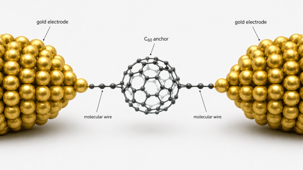
One important area is single-molecule electronics. In a molecular junction, a molecule is placed between two electrodes, often gold electrodes. The anchoring group that connects the molecule to the metal surface strongly affects conductance and reproducibility.
Traditional anchoring groups such as thiols and amines are widely used, but their conductance can vary depending on contact geometry. C60 has been studied as an alternative molecular anchor because it can interact strongly with gold surfaces and provide a robust contact motif in certain junction designs.
This does not mean C60 is universally superior for all molecular wires. Molecular conductance depends on electrode material, contact geometry, molecular backbone, orbital alignment, measurement method, and environment. But C60 remains important because it gives researchers a distinctive way to study molecule-electrode coupling.
Organic field-effect transistor memory, or OFET memory, is another area where fullerene materials have been studied. In these devices, fullerene derivatives may act as charge-trapping sites, floating-gate components, or photosensitive elements in hybrid organic systems.
PCBM and related fullerene derivatives can interact with polymer matrices and organic semiconductors in ways that influence charge storage and release. This makes them useful in experimental nonvolatile memory devices and photomemory systems.
The practical importance is not that all fullerene-based OFET memories are ready for commercial memory chips. The importance is that C60 and PCBM-type materials offer molecular tools for controlling charge trapping, photoresponse, and interfacial electronic behavior in organic semiconductor devices.
For researchers, this creates a bridge between material chemistry and device physics. The same electron-accepting behavior that made fullerenes important in OPV also makes them useful in memory and charge-transfer studies.
C60 also appears in one-dimensional nanotechnology through so-called peapod structures, where fullerene molecules are encapsulated inside single-walled carbon nanotubes. These structures are often written as C60@SWCNT.
In C60 peapods, fullerene molecules form a chain inside the nanotube. This creates a confined nanoscale system where carbon nanotube electronic behavior and fullerene electronic behavior can interact. Studies have explored charge transfer, electronic modification, optical response, and nanoscale transport in these structures.
Ultrafast spectroscopy studies have reported rapid photoinduced charge transfer between SWCNTs and C60, showing that these hybrid carbon nanostructures can support fast electronic interactions. These findings are relevant to fundamental molecular electronics and nanoscale optoelectronic research.
For industrial application, peapods remain more specialized than conventional C60 or PCBM OPV materials. They are better understood as frontier research structures rather than routine commercial electronic raw materials.
Transient electronics are devices designed to disappear, degrade, or become inactive after a defined operating period. This field is relevant to temporary sensors, environmental devices, and certain biomedical or disposable electronics concepts. Any biomedical use must be discussed carefully and requires separate safety and regulatory evaluation.
PCBM has been studied in transient electronic systems because fullerene derivatives can influence photochemical degradation in polymer matrices. In PS:PCBM systems, UV exposure and water can trigger degradation behavior, allowing the material system to change or disintegrate under defined conditions.
This is a different use of fullerene chemistry from OPV. In OPV, the goal is stable charge separation and long device lifetime. In transient electronics, the goal may be controlled instability after a trigger. The same fullerene derivative can therefore have different value depending on the device concept.
This contrast shows why fullerene materials should be described by application context. A property that is useful in one device may be a liability in another. UV response, oxygen sensitivity, charge transfer, and morphology must all be understood within the actual device architecture.
The movement from innovation to industrialization requires solving several linked problems. The first is efficiency. OPV modules must reach performance levels suitable for their target applications, even if they do not match silicon in peak efficiency.
The second is stability. Organic semiconductors can be sensitive to oxygen, moisture, heat, ultraviolet light, and morphology changes. Encapsulation and material design must work together to limit degradation.
The third is scalable processing. Spin-coated small cells are valuable for research, but industrial production needs methods such as blade coating, slot-die coating, printing, evaporation, or roll-to-roll compatible processes. The active layer must remain uniform and functional across larger areas.
The fourth is material reproducibility. OPV and molecular electronic devices are sensitive to impurities, energy levels, film morphology, and interfacial behavior. For research and scale-up, material identity and consistency matter.
The fifth is realistic application targeting. OPV may be strongest in markets where flexibility, low weight, transparency, or low-temperature processing are valuable. Molecular electronics may remain closer to research, sensing, memory, or specialized nanoscale devices before broader commercial deployment.
For fullerene materials, the industrialization of organic photovoltaics and molecular electronics means that C60 and C70 should be evaluated as precision research materials, not generic carbon powders. Their value depends on chemical identity, purity, morphology behavior, solubility, electronic properties, and compatibility with the target device system.
C60 may be relevant for organic electronics, vacuum-deposited devices, molecular junctions, and interfacial studies. C70 and PC71BM may be considered where different optical absorption or electronic behavior is useful. PC61BM remains historically important and still relevant in selected solution-processed systems, ternary blends, and charge-transfer studies.
Material selection should not be simplified into “C70 is better than C60” or “non-fullerene acceptors replace all fullerenes.” In real device research, selection depends on donor material, acceptor system, solvent, deposition method, desired morphology, device stack, and stability target.
For research teams and advanced material companies, the most useful approach is to begin with the device architecture and work backward to the material requirement.
If you are evaluating fullerenes for organic photovoltaics or molecular electronics, define the device context first. A vacuum-deposited C60 layer, a PCBM-based BHJ active layer, a C70 derivative acceptor system, a molecular wire junction, and a charge-trapping OFET memory all require different material thinking.
For general research reference, you may review Fullerene C60 product information, Fullerene C70 product information, or contact The Fullerene to discuss material identity, purity options, sample availability, and application-specific requirements.
Organic photovoltaics are solar cells that use organic semiconductor materials to absorb light and generate electricity. They are studied for lightweight, flexible, semi-transparent, and solution-processable solar applications.
C60 is important because it is an electron-accepting fullerene molecule with a long history in organic electronics. It has been used in vacuum-deposited devices, electron-transport research, and as the parent structure for soluble derivatives such as PC61BM.
PC61BM is a soluble C60 derivative widely used in early solution-processed bulk heterojunction OPV research. Its improved solubility helped make polymer:fullerene solar cells easier to fabricate by solution processing.
C60 contains 60 carbon atoms and has a highly symmetrical spherical structure. C70 contains 70 carbon atoms and has a more elongated molecular geometry. These structural differences can lead to different optical and electronic behavior. Selection depends on the application and device system.
Non-fullerene acceptors have become dominant in many high-efficiency OPV systems, but they do not make fullerene materials irrelevant. C60, C70, PCBM derivatives, and fullerene-based materials remain useful in reference systems, interfacial research, ternary blends, molecular electronics, and charge-transfer studies.
The main challenge is translating small-cell performance into stable, large-area modules. This requires scalable coating, morphology control, low interconnect loss, stable encapsulation, and reproducible material quality.
Molecular electronics studies how molecules or molecular assemblies can perform electronic functions such as charge transport, switching, memory, sensing, or nanoscale interconnection.
C60 is studied in molecular wires because it can interact strongly with metal electrodes such as gold and may provide a useful molecular contact motif in single-molecule junctions. Conductance still depends on contact geometry, molecular backbone, and measurement conditions.
OPVs are not generally better than silicon in peak efficiency. Their value lies in different application advantages, including flexibility, low weight, thin-film format, semi-transparency, and low-temperature processing potential.
[1] R. Basu et al., “Large-area organic photovoltaic modules with 14.5% certified world-record efficiency,” Joule, 2024. The paper reports a 204 cm² OPV module with 14.5% certified efficiency and discusses CFD-supported blade coating and FEM-supported module optimization. Source
[2] PV Magazine, “Large area organic PV module achieves world record efficiency of 14.5%,” March 8, 2024. The report states that the module measured 143 mm × 143 mm, had an active area of 204.11 cm², and was certified by Fraunhofer ISE. Source
[3] S. Yuan et al., “Progress in research on organic photovoltaic acceptor materials,” RSC Advances, 2025. The review summarizes fullerene and non-fullerene acceptor materials for organic solar cells. Source
[4] G. Zhang et al., “Nonfullerene Acceptor Molecules for Bulk Heterojunction Organic Solar Cells,” Chemical Reviews, 2018. The review discusses the emergence of non-fullerene acceptors as alternatives to fullerene derivatives in OPV research. Source
[5] L. Venkataraman et al., “Fullerene-Based Anchoring Groups for Molecular Electronics,” Journal of the American Chemical Society, 2008. The study discusses C60 as an anchoring group in molecular electronics and its interaction with gold surfaces. Source
[6] ACS Applied Materials & Interfaces, “Phototriggerable Transient Electronics via Fullerene-Mediated Degradation.” The paper reports PCBM-mediated phototriggerable transient behavior in polymer electronic systems. Source
[7] A. M. Dowgiallo et al., “Ultrafast spectroscopic signature of charge transfer between single-walled carbon nanotubes and C60,” PubMed record, 2014. The study reports ultrafast photoinduced charge transfer between SWCNTs and C60. Source
[8] PubChem, “Fullerenes.” PubChem provides chemical identity and structure information for Fullerene C60. Source
For B2B procurement of Fullerene C60 (Pure), 99.95% Purity, No metallic residue, buyers should confirm target purity, required quantity, application, destination country, COA, MSDS/SDS, packaging, storage conditions, and shipping requirements before requesting a formal quotation.
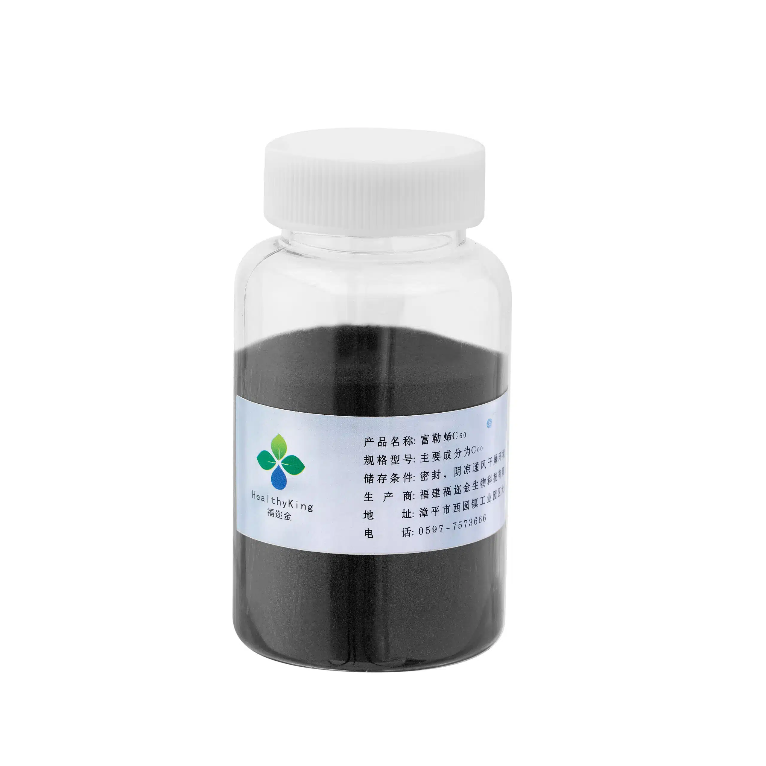
High-purity fullerene C60 is a highly refined nanomaterial designed specifically for the most demanding scientific and industrial applications. This ultra-pure form ensures…
Request product specifications, batch-specific COA, MSDS/SDS, sample availability, packaging details, and international shipping information before confirming your order.
Request DocumentsSubmit your product, purity, quantity, application, destination country, and documentation requirements. Our team will help confirm availability, COA, MSDS/SDS, packaging, and quotation details.