
XCT Insights
Stay Updated
Fullerene research, applications and company updates, delivered occasionally.
Latest from XCT
View all


A perovskite–silicon tandem solar cell reported in 2026 reached a measured power conversion efficiency of 33.33% and a certified efficiency of 32.89% on an active area of approximately 1 cm². The result is technically important, but its cause must be described accurately. The principal innovation was not a newly demonstrated “metal-free” grade of Fullerene C60. It was a peak-selective passivation strategy designed to suppress electrical leakage at the sharp pyramid peaks of an industrially textured silicon bottom cell.[1]
C60 may still form an important electron-transporting contact in the perovskite top-cell stack, as it does in many inverted perovskite and perovskite–silicon tandem architectures. However, the presence of C60 in a high-efficiency device does not mean that C60 purity alone produced the efficiency result. Nor does the published record establish that completely metal-free C60 is a prerequisite for reaching 33% efficiency.
This distinction matters for researchers and photovoltaic material teams. It allows the result to inform C60 qualification without converting a device-level interface-engineering study into an unsupported raw-material claim. The correct question is not whether a supplier can attach “metal-free” to a C60 product. It is which C60 attributes can affect deposition, interface quality and process repeatability, and which analytical evidence is needed to evaluate those attributes.
The 2026 study, published in Matter, addressed a geometric and electrical problem found when perovskite top cells are fabricated on industrially textured silicon bottom cells. Commercial crystalline-silicon surfaces are commonly textured with microscopic pyramids to improve optical performance. These structures are useful for light management, but their high-curvature peaks make uniform deposition of the upper functional layers difficult.
If the perovskite and transport layers become too thin or discontinuous around a pyramid peak, the region can develop an increased local electric field or form a leakage pathway. A small number of these weak locations can reduce fill factor, lower effective voltage and accelerate local degradation even when the rest of the device is well formed.
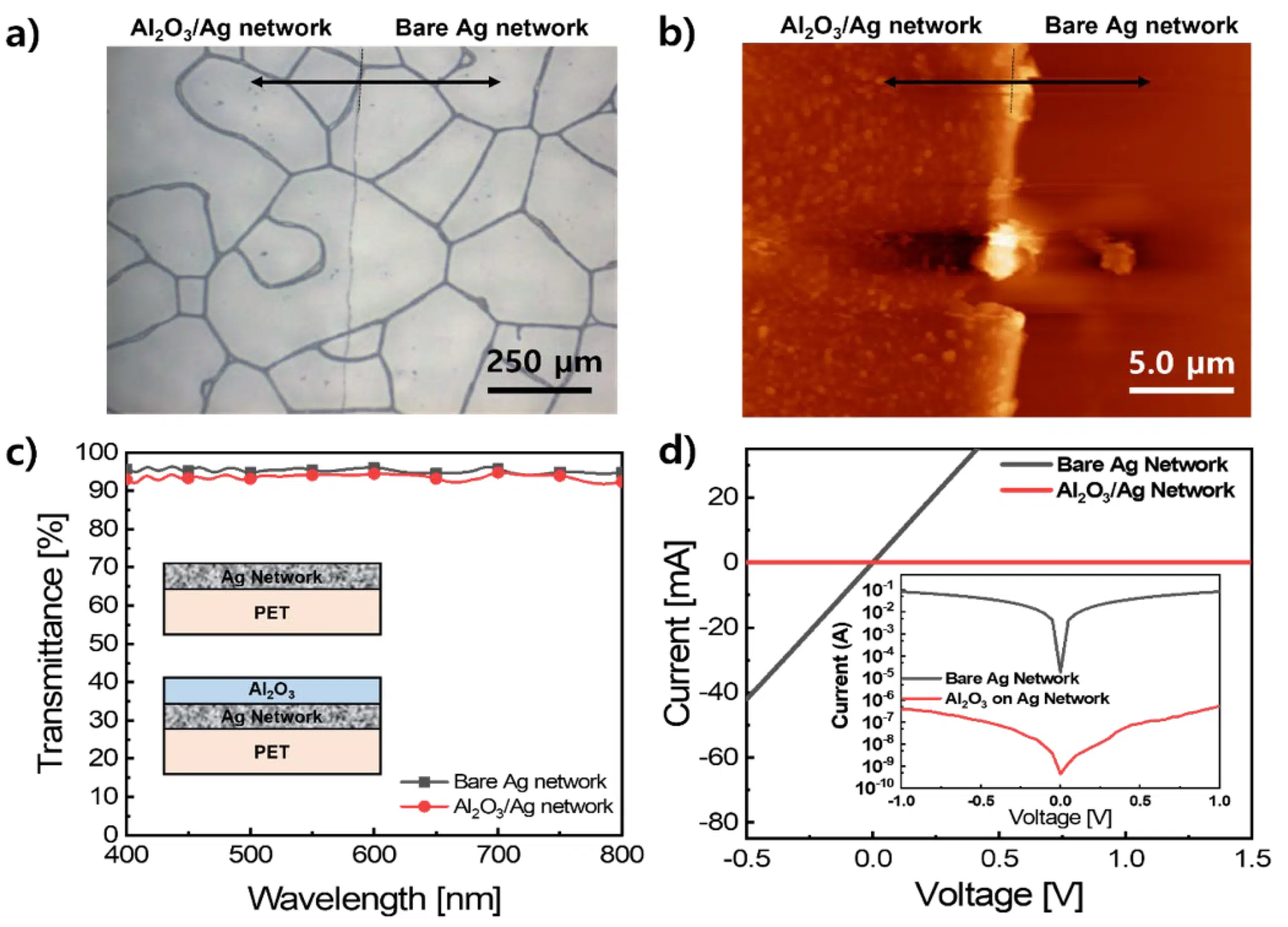
To address this problem, the research team developed a peak-selective passivation strategy. Polystyrene nanospheres were used as a self-aligned template so that a thin aluminum oxide layer could be deposited selectively at the pyramid apex regions. After the template was removed, the Al₂O₃ remained at the locations most susceptible to electrical leakage.
The resulting device reached 33.33% measured efficiency and 32.89% certified efficiency over an active area of about 1 cm². The authors also reported that the device retained approximately 90% of its initial efficiency after 1,000 hours of continuous operation under the stated test conditions.[1][2]
These figures should be reproduced with their qualifications. The measured value and certified value are different, and neither should be described as a universal 33.33% threshold. At the time of the institutional announcement, higher perovskite–silicon tandem records had already been reported, so the significance of the paper lies in its device architecture, compatibility with industrial texture and leakage-control strategy rather than in establishing a new minimum efficiency requirement.[2]
The study does not support the claim that completely metal-free C60 was responsible for the reported efficiency. Its central experimental variable was the selective Al₂O₃ passivation of the silicon pyramid peaks. The public abstract and institutional description do not identify C60 elemental purity as the mechanism responsible for the efficiency improvement.
This does not mean that C60 quality is irrelevant. It means that the evidence must be assigned to the correct level of the device.
A tandem cell contains many coupled components: the silicon bottom cell, recombination junction, hole-selective contact, wide-bandgap perovskite absorber, passivation layers, electron-selective contact, transparent electrode, optical layers and metal contacts. A performance change can arise from any of these components or from their interactions. When a study modifies one structural feature and holds the remaining process as constant as practicable, the demonstrated effect belongs primarily to that modified feature.
It is therefore not scientifically valid to infer the following chain without direct evidence:
The device used C60; the device reached more than 33% efficiency; therefore the C60 must have been entirely metal-free; therefore entirely metal-free C60 is required for all devices above 33%.
Each step introduces an unsupported assumption. A defensible article should instead separate the published device result from the broader evidence concerning C60 source quality.
In many monolithic perovskite–silicon tandem cells, the perovskite top cell uses an inverted, or p–i–n, architecture. Starting from the bottom side of the perovskite subcell, a simplified stack can include a hole-selective layer, a wide-bandgap perovskite absorber, an electron-transport layer, a buffer or protective layer and a transparent conductive electrode.
C60 is widely used as the electron-transport layer in this type of device. It has electron-accepting character, suitable electron-transport properties and energy levels that can support electron extraction while restricting holes. Thermal evaporation can also form thin C60 layers without exposing the underlying perovskite to a liquid solvent.
These advantages explain why thermally evaporated C60 has been described in peer-reviewed research as a near-ubiquitous ETL in state-of-the-art p–i–n perovskite-based solar cells.[3]
However, the ETL does not operate independently. Its performance depends on:
For a deeper treatment of the material’s function, see C60 electron transport layers in perovskite–silicon tandem solar cells.
C60 should not be described as automatically passivating every perovskite surface or eliminating all charge-recombination pathways. The interface can support electron extraction, but it can also become a major source of voltage loss.
Studies of inverted perovskite cells have shown that non-radiative recombination frequently occurs at the perovskite/C60 interface. Proposed contributors include interfacial defects, unfavorable local energy alignment, charge-transfer states, chemical interactions and ion accumulation.[4]
A 2025 study of perovskite–silicon tandem cells reported substantial quasi-Fermi-level splitting losses after C60 deposition on an untreated or incompletely passivated perovskite surface. The researchers reduced these losses using a bilayer AlOx/PDAI2 interface treatment, demonstrating that the quality of the interface surrounding C60 can be as important as the presence of C60 itself.[5]
This observation changes how C60 should be discussed in high-efficiency devices. C60 is not a standalone efficiency additive. It is one component of an engineered electron-selective contact. Its contribution can only be understood together with perovskite surface preparation, interlayers, deposition conditions and the complete energy-loss budget.
Although the 32.89%-certified peak-passivation study does not establish a metal-free requirement, independent research does show that C60 source quality can affect repeated thermal evaporation and device reproducibility.
In a 2024 Nature Communications study, researchers compared commercial as-received C60 with further sublimed material. The as-received source could coalesce during repeated evaporation, while additional sublimation reduced this behavior. The study associated the coalescence with oxygen in the initial C60 powder and linked it to deep states and declining device performance during repeated processing.[3]
Using further purified C60, the researchers obtained reproducible perovskite–silicon tandem performance over eight repeated evaporation processes. One device achieved a certified efficiency of 30.9%. This is strong evidence that source preparation and repeated-use behavior can matter in a thermal evaporation workflow.
It is not evidence that a single HPLC number guarantees device performance. Nor is it evidence that all undesirable behavior is caused by transition metals. In that study, oxygen-related source behavior and sublimation purification were central to the result.
The material qualification question should therefore be broadened from “Is the C60 metal-free?” to:
The site’s guide to C60 HPLC purity analysis explains why chromatographic purity answers only part of this qualification problem.
Elemental impurities can matter in electronic materials, but their effect must be established through appropriate analysis and device evidence. Different elements, chemical forms, particle sizes and concentrations may behave differently. A dissolved ionic species is not equivalent to an embedded inorganic particle, and a surface contaminant is not necessarily equivalent to an impurity distributed throughout the source powder.
Potential concerns may include:
These are legitimate reasons to control elemental impurities. They do not justify stating that any detectable amount of nickel, cobalt, iron or copper automatically prevents a tandem cell from reaching 33% efficiency.
A meaningful low-metal specification should identify the elements, the analytical technique, the sample-preparation method, the units and the reporting limits. ICP-MS or ICP-OES may be used for selected elemental measurements, but the result must be connected to the actual batch. A combustion-based or nominally catalyst-free production route cannot by itself establish that the final powder contains no trace metals.
Absolute terms such as “zero metals,” “completely metal-free” and “intrinsically free of heavy metals” should therefore be avoided unless they are rewritten as bounded process statements or batch-specific analytical results.
High-performance liquid chromatography can separate and quantify chromatographically detectable fullerene species under a defined method. It is useful for evaluating C60 relative to C70, higher fullerenes and certain organic fullerene-related impurities.
It does not normally quantify total elemental impurities. A sample described as 99.95% by HPLC area may still contain substances that:
For photovoltaic material evaluation, separate questions may require separate methods:
| Question | Possible analytical approach |
|---|---|
| Is C60 the dominant chromatographically detectable fullerene? | HPLC with a suitable column, detector and calculation method |
| Does the sample have the expected molecular identity? | Mass spectrometry and complementary spectroscopy |
| Are selected elements present above specified limits? | ICP-MS, ICP-OES or another validated elemental method |
| Are volatile process solvents present? | Headspace GC or GC-MS |
| Does the source behave consistently during heating and evaporation? | Thermal analysis, evaporation trials, source-residue inspection and film characterization |
| Does the material support reproducible devices? | Controlled device fabrication across batches and repeated evaporation cycles |
No single result should be expanded beyond the property it actually measures.
For perovskite photovoltaic research, “high-purity C60” is most useful when treated as a multidimensional material definition rather than a single percentage.
The HPLC method should separate the fullerene-related components relevant to the intended specification. The report should state whether the percentage represents area normalization, calibrated assay or another calculation.
A source intended for thermal evaporation should be evaluated under the actual temperature, vacuum and reuse conditions. Powder appearance alone cannot predict whether the material will coalesce, form residue, change composition or produce a consistent deposition rate.
If specific metals are relevant to the device process, they should be named and measured. “No metallic residue” is not a complete specification without elements, units, method and limits.
The evidence linking oxygen-containing source material to repeated-evaporation behavior makes storage and handling relevant. Packaging should limit uncontrolled exposure appropriate to the established material sensitivity, but the exact storage requirement should be supported by stability or process data rather than generic language.
A single high-performing batch does not establish manufacturing consistency. Research and scale-up teams should compare deposition rate, source residue, film morphology, electrical properties and device metrics across multiple batches.
A practical qualification program should begin with the device process and its likely failure modes.
Specify whether C60 will be thermally evaporated, deposited from solution or integrated through another method. A grade suitable for solution research is not automatically qualified for repeated vacuum evaporation.
Identify which variables are most likely to affect the program: fullerene composition, volatile residue, oxygen-related source behavior, selected metals, moisture exposure, thermal residue, particle contamination or batch variability.
A 99.95% value should be accompanied by its method and calculation basis. Elemental results should identify the measured elements and reporting limits. Statements such as “not detected” should never be interpreted without the limit of detection or quantitation.
For a source that will be reused, examine several sequential cycles. Monitor deposition rate, source morphology, residue, film uniformity and device performance rather than relying on a single first-cycle result.
Use controlled device comparisons. When an interlayer, passivation treatment or substrate texture is changed, retain the same C60 batch where possible. When the C60 batch is changed, hold the interface treatment and deposition process constant. This prevents an improvement caused by one variable from being assigned to another.
The peak-selective passivation study provides three useful lessons for C60 users, even though it does not demonstrate a metal-free requirement.
First, high-efficiency tandem performance depends on local interface quality. Thin regions, sharp features and incomplete coverage can dominate device losses. A nominal material purity percentage cannot compensate for a defective geometry or poorly engineered contact.
Second, industrially relevant substrates create different challenges from flat laboratory substrates. Material qualification must eventually be performed in the intended texture, area and deposition process.
Third, C60 should be evaluated as part of a complete electron-selective interface. Source quality, perovskite passivation, film continuity, energy alignment and upper-electrode processing all contribute to the final result.
For teams moving from exploratory cells toward repeatable tandem fabrication, The Fullerene can support evaluation of Fullerene C60 grades for research and electronic-material workflows. XCT should only present batch purity, elemental results and processing suitability according to the documentation available for the specific material.
Discuss C60 requirements for a perovskite ETL process
The published study does not establish that conclusion. Its central innovation was selective Al₂O₃ passivation of leakage-prone pyramid peaks on an industrially textured silicon bottom cell. C60 may have been part of the electron-transport stack, but the reported efficiency improvement was not demonstrated as a consequence of metal-free C60.
The study reported a measured efficiency of 33.33% and a certified efficiency of 32.89% for a device with an active area of approximately 1 cm². The two values should not be presented as interchangeable.
C60 is widely used as an electron-transport layer in inverted perovskite architectures because it can support electron extraction and hole blocking and can be deposited as a thin film by thermal evaporation. Its performance depends on the perovskite/C60 interface and the surrounding device layers.
No. HPLC purity describes chromatographically detected components under a defined method. Device efficiency also depends on source evaporation behavior, interface passivation, film morphology, substrate texture, energy alignment, electrodes and the full fabrication process.
No. A route that does not intentionally use a metal catalyst can reduce one possible contamination source, but the final material must be tested if an elemental specification is required. Results should identify the tested elements, method, units and reporting limits.
Relevant information may include the chromatographic method, purification history, selected elemental results, volatile residue, storage conditions, thermal behavior, source coalescence or residue, deposition consistency and device performance across repeated evaporation cycles.
For B2B procurement of Fullerene C60 (Pure), 99.95% Purity, No metallic residue, buyers should confirm target purity, required quantity, application, destination country, COA, MSDS/SDS, packaging, storage conditions, and shipping requirements before requesting a formal quotation.
High-purity fullerene C60 is a highly refined nanomaterial designed specifically for the most demanding scientific and industrial applications. This ultra-pure form ensures…
Request product specifications, batch-specific COA, MSDS/SDS, sample availability, packaging details, and international shipping information before confirming your order.
Request DocumentsSubmit your product, purity, quantity, application, destination country, and documentation requirements. Our team will help confirm availability, COA, MSDS/SDS, packaging, and quotation details.